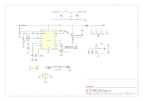
Just a quick post this week. I've finally gotten around to doing the PCB for my power supply and I thought I'd talk about grounding. I'm not claiming to be an expert, I'm just trying to follow best practice and all the bits and pieces I picked up from reading textbooks and app notes. As usual, university basically teaches you nothing about this. You're told that the little ground symbol is zeros volts and you can dump current into it and everything will be fine, but that quickly starts to fall apart in real world situations.
 |
| Kicad power supply schematic |
What you consider to be a zero impedance connection in a schematic has
resistance, inductance, and capacitance. This means that if your
circuit requires large currents or high frequency to operate, that
ground will no longer be zero volts. One strategy to deal with this is
to segregate grounds into different types and then combine them at a
central point via a star grounding system. This means that individual subsystems
will operate with a common ground. It also allows you to treat each
ground separately. You can use wide tracks for high current grounds,
or make sure that you have tight ground loops on high frequency sections
to avoid EMI problems. Either way you need a way to deal with this
when designing your PCB.
In the schematic above I've created three different grounds to help manage these issues. An power input ground, a power output ground, and a signal ground. The power grounds are for high current parts of the switch mode converter, and the signal ground is for the controller and low current signal conditioning circuits. I think I have everything segmented correctly, I guess I'll find out when it comes time to test the circuit.
So you have your separate grounds, how do you connect them. If you connect them all to a ground node, Kicad will treat them all as one net and you loose the logical separation of them. The way to get around this is to create a component called a net-tie or pavilion ground. It's basically a component with multiple nodes that's made of copper to connect all the nets. It allows all the grounds to come together at one point and still keep the nets logically separated.
 |
| Net Tie |

And I guess this never happened when you later realised that you have a problem when you get to PCB the side.
ReplyDeleteNope, it's easy to do. In the footprint editor just put a graphical line on the F.Cu layer to tie the two pads together. (KiCad doesn't check DRC on graphics)
Delete